AUCAOS Online Seminars
Due to the cancellation of many scientific conferences, the AUCAOS committee is pleased to host online seminars on the first Wednesday of every month until normal conferences can resume.
Screen recordings of past seminars are available to view below.
Wednesday 2 March 2022
Seminar 1
1:00 - 1:25pm AEST
Materials Intermixing and the Dipole Formation at the active Layer/Conjugated Polymer P(NDI3N-T-Br) Interface
Amira R Alghamdi1, Jonas M Bjuggren1, Mats R. Andersson1, and Gunther G. Andersson1*
1,* Flinders Institute for Nanoscale Science and Technology, Flinders University, GPO Box 2100 Adelaide SA 5001, Australia
Interfacial engineering using interface layers has been identified as an essential approach for maximizing power conversion efficiency (PCE) of polymer solar cells (PSCs) by optimizing the charge transport between the active layer and the charge extracting electrodes through aligning the energy levels between the layers in a device. The properties of an interface layer have to allow for the transport of one of the charge carriers and at the same time block the other. As an example, the interface layer helping to extract the electrons from the active layer should block the transport of the holes to the same interface layer. P(NDI3N-T-Br) polymer was used as a cathode interface layer in inverted organic solar cells (OSCs) fabricated using poly[2,3-bis(3- octyloxyphenyl)quinoxaline-5,8-diyl-alt-thiophene-2,5-diyl] (TQ1) and poly[[N,N'-bis(2-octyldodecyl)-naphthalene-1,4,5,8-bis(dicarboximide)-2,6-diyl]-alt-5,5'-(2,2'-bithiophene)] (N2200) as the donor and acceptor materials, respectively. The aim of the work is to determine the position of the energy levels of P(NDI3N-T-Br) to those of the materials forming the active layer, resulting in a physical and electronic model of the interface region. We show that these quantities can be derived from the electron spectroscopy data when a full component analysis of the valence electron spectra is conducted. The valence electron spectroscopy technique shows that a dipole formed at the interface between TQ1, and P(NDI3N-T-Br) blocks the transfer of holes from the active layer to the P(NDI3N-T-Br). However, the transfer of electrons from N2200 is facilitated.
Seminar 2
1:25 - 1:50pm AEST
Investigating the long-term stability of organic light emitting diodes by Rutherford backscattering technique
Tengfei Qiu
Centre for Organic Photonics & Electronics, School of Chemistry and Molecular Biosciences, The University of Queensland, Brisbane, QLD 4072, Australia.
Phosphorescent organic light emitting diodes (P-OLEDs) are a promising display technology due to the high colour purity and quantum efficiency. The long-term stability is one of the major issues for these devices. In a typical P-OLED structure, the emissive layer containing phosphorescent molecules is sandwiched by several electron transport layers and hole transport layers. Physical changes in the film structure caused by interlayer material diffusions dramatically changed the photoelectric properties. Obvious changes in material density and thickness under rapid annealing conditions to temperatures higher than the glass transition temperatures of the materials can be detected by neutron reflectometry (NR). Corresponding changes in emitting properties can be reflected in the photoluminescent (PL) spectra. However, performance degradations happen in the course of normal operational conditions for display applications, where temperatures higher than room temperature and lower than 60 ° C are more likely to be encountered. Under such mild conditions, the minor changes in material density and thickness are difficult to detect. There is a lack of methods to detect such diffusion and further to clarify the causes of the changes in the PL spectra. Here, we use the Rutherford backscattering technique, which is able to detect the distribution of heavy metal element of phosphorescent molecules in the organic matrix to study the role of the diffusion of the phosphorescent molecules on the long-term stability of OLED devices. The work provides a new approach for investigating the performance degradation mechanism of OLEDs
Wednesday 3 December 2021
Seminar 1
1:00 - 1:25pm AEST
Synthesis of 2D nanomaterial from waste and its application in opto-electronic and sensing
Amandeep Singh Pannu
Queensland University of Technology
The study investigates an end-to-end solution for developing carbon based 2D semiconductor nanomaterial or quantum dots from carbon rich bio-waste and demonstrates its application into thin film devices and solution based optical sensing. The presentation is divided into two parts. The first part will share the outcome of study, which explores the synthesis method to produce such high performing quantum dot material and tune its opto-electronic properties via surface engineering based on its application either in sensing or active/charge transporting layer in light emitting diodes and solar cell devices. The second part of the presentation will share the insights on how to apply this synthesized material successfully into hybrid devices.

Seminar 2
1:25 - 1:50pm AEST
Harnessing triplet excitons in organic solid-state lasers
Atul Shukla
The University of Queensland
Organic light-emitting device technology has been shown promising for a paradigm shift from organic light-emitting diodes (OLEDs) to organic laser diodes (OLDs).[1] While significant progress has been made for organic semiconductors emitting in the blue–green region of the visible spectrum, organic laser dyes with low-energy emission (>600 nm) still suffer from high amplified spontaneous emission (ASE) thresholds and low external quantum efficiencies (EQEs) in devices under high current densities.[2, 3] In this presentation, low ASE thresholds and efficient electroluminescence (EL) from a solution-processable organic laser dye dithiophenyl diketopyrrolopyrrole (DT-DPP) will be shown. A low ASE threshold of 4 µJ cm-2 with λASE ≈ 620 nm will be presented by making constructive use of triplet excitons via doping DT-DPP in a green-emitting host matrix that exhibits thermally activated delayed fluorescence (TADF). A high EQE of 7.9% of fabricated OLEDs due to the efficient utilization of triplet excitons is demonstrated. Finally, the critical role of reverse intersystem crossing rate in achieving lasing under electrical pumping from such TADF-assisted fluorescent systems will be discussed using transient EL studies.[4]
References:
[1] A. S. D. Sandanayaka, et al., Appl. Phys. Express, 12, 061010 (2019).
[2] M. Mamada, et al., Adv. Funct. Mater., 28, 1802130 (2018).
[3] A. Shukla, et al., Adv. Opt. Mater., 8, 1901350 (2020).
[4] A. Shukla, et al., Adv. Funct. Mater., 31, 2009817 (2021).
Wednesday 3 November 2021
1:00 - 1:25pm AEST
High Efficiency Deep Blue OLEDs
Jang-Joo Kim
Seoul National University, Korea
JooAm Co.
The efficiency of organic light emitting diodes has been significantly improved during the last several years by developing phosphorescent and TADF emitters with high horizontal emitting dipole orientation and high PLQY along with the development of device structure with excellent charge balance to get EQE reaching almost 40%, corresponding to almost the theoretical limit of the efficiency. The most important remaining issue is the development of deep blue OLEDs. In this talk, we will firstly present a theoretical model to analyze the degradation mechanism of OLEDs and application of the model to blue OLEDs. Then we will talk about a strategy to realize deep blue TADF OLEDs with the EQE of 28% and CIE y value of 0.09 by narrowing the emission spectrum of blue emitting TADF emitters along with high horizontal emitting dipole orientation. Lastly, we will discuss on deep blue OLEDs utilizing triplet-triplet annihilation (TTA) process based on anthracene derivatives. For blue-emitting anthracene derivatives, the theoretical maximum contribution of TTA to emissive singlet excitons is 15%, which is insufficient for high-efficiency fluorescent devices. In this study, we realised a TTA contribution of nearly 25% using an anthracene derivative, breaking the theoretical limit. As a result, efficient deep-blue TTA fluorescent devices were developed, which exhibited maximum external quantum efficiencies of 10.2%. A theoretical model will be presented to explain the experimental results considering both the TTA and RISC to a singlet state from a high level triplet state formed by the TTA process.
Wednesday 6 October 2021
Seminar 1
1:00 - 1:25pm AEST
Rivers of light - ternary exciplex blends for high efficiency solution-processed red phosphorescent organic light emitting diodes
Jaber Saghaei,1 Steven M. Russell,1 Hui Jin,1 Paul L. Burn,1* Almantas Pivrikas2, Paul E. Shaw1
1Centre for Organic Photonics & Electronics (COPE), School of Chemistry and Molecular Biosciences, The University of Queensland, Brisbane, Queensland 4072, Australia
2School of Engineering and Information Technology, Murdoch University, Perth, Western Australia, 6150, Australia
* p.burn2@uq.edu.au
Red-emitting organic light-emitting diodes (OLEDs) are important for displays and lighting, with the latter benefiting from solution processable materials, which would enable low embedded energy, scalable fabrication. Herein we describe the effect of annealing and phase separation on the performance of solution-processed OLEDs incorporating a light emitting layer composed of the exciplex host, m-MTDATA:OXD-7, and a red phosphorescent light-emitting dendrimer, Ir(tDCpq)3. Solution-processed OLEDs containing an annealed emissive layer with a low dendrimer concentration (2 wt%) were found to have the best performance, which was higher than the device in which the light emitting layer was not annealed. The improvement in performance of the annealed device was ascribed to improved charge mobility within the emissive layer caused by phase separation of the OXD-7. The OLEDs containing annealed m-MTDATA:OXD-7:(2 wt%) Ir(tDCpq)3 had maximum current, power and external quantum efficiencies of 17.9 cd/A, 19.4 lm/W, and 14.8±0.6%, respectively. The fact that the maximum EQE of 14.8% was larger than that expected based on the PLQY and the normal out-coupling efficiency of 20% from a bottom-emitting devices was determined to arise from the different pathways of exciton formation under photoexcitation and charge injection.
Wednesday 1 September 2021
Seminar 1
1:00 - 1:25pm AEST
Understanding the formation and morphology of organic semiconductor thin films at the atomic level
Audrey V. Sanzogni
The University of Queensland
Functional thin films composed of organic semiconductors are transforming opto-electronic devices ranging from light weight flexible solar cells, lighting and displays to the latest in low-cost tuneable sensor materials. The key active layers in these devices are not only amorphous but often only tens of nanometre thick meaning the morphology of the material is dominated by interfacial effects and the properties of the materials depend not only on the chemical composition, but the manner of deposition and post-manufacturing processes. Furthermore, while experimental studies on amorphous systems can provide information on bulk or averaged properties, the performance of a specific device in terms of efficiency and life-time are often dominated by variations in the local morphology. To advance the utility of organic thin film devices, we need to understand how morphology relates to performance in atomic detail.
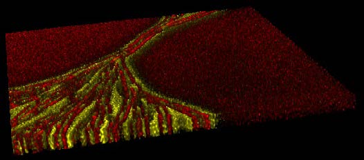
In my talk I will show how atomistic molecular dynamics simulations in which different manufacturing processes such as vacuum deposition1 and solution processing2 are reproduced in detail are providing novel insights into how morphology affects the performance of real devices. The predictive power of these models will be demonstrated as well as how elements such as the aggregation of guest molecules in a host matrix and the potential of solvent remaining in a thin film after solution deposition (Figure 1) are providing key insights into the function and properties of organic thin films.

Figure 1: Snapshots of a solution processing simulation over time and the resulting thin film
1. Lee, T.; Sanzogni, A.; Zhangzhou, N.; Burn, P. L.; Mark, A. E., Morphology of a Bulk Heterojunction Photovoltaic Cell with Low Donor Concentration. ACS Appl. Mater. Interfaces 2018, 10 (38), 32413-32419.
2. Lee, T.; Sanzogni, A. V.; Burn, P. L.; Mark, A. E., Evolution and Morphology of Thin Films Formed by Solvent Evaporation: An Organic Semiconductor Case Study. ACS Appl. Mater. Interfaces 2020, 12 (36), 40548-40557.
Seminar 2
1:25 - 1:50pm AEST
Balanced Hole and Electron Transport in TCTA:Ir(ppy)3 Blends as Determined by Photo-MIS-CELIV
Mile Gao1, Paul L. Burn,1* Almantas Pivrikas2
1Centre for Organic Photonics & Electronics (COPE), School of Chemistry and Molecular Biosciences, The University of Queensland, Brisbane, Queensland 4072, Australia 2Physics department, Murdoch University, Perth, Western Australia, 6150, Australia * p.burn2@uq.edu.au
Balanced charge injection and transport in organic light emitting diodes (OLEDs) is essential for highly efficient devices with small efficiency roll-off at high luminance. However, there are few reports on the measurement of charge mobility within the blend emissive layer of an OLED. In this presentation, we show that photoexcitation in conjunction with Metal-Insulator-Semiconductor Charge Extraction with Linearly Increasing Voltage (photo-MIS-CELIV) can be used to determine the hole and electron mobilities of the emissive blend layer in a single device architecture. We demonstrate the technique by studying the commonly used emissive blend of fac-tris[2-phenylpyridinato-C2,N]iridium(III) [Ir(ppy)3] and tris(4-carbazoyl-9-ylphenyl)amine (TCTA) as well as neat TCTA and Ir(ppy)3 films. It was found that Ir(ppy)3 and its blend films with TCTA have measurable electron mobilities and critically they are of similar magnitude as their hole mobilities, irrespective of the Ir(ppy)3 doping ratio. Such balanced charge mobility suggests that the transport of both holes and electrons occurs mostly on the Ir(ppy)3 guest molecules in the blend. Additionally, we demonstrate that photo-MIS-CELIV can be used to measure the quantum efficiency of exciton dissociation in organic semiconductor thin films.
Wednesday 4 August 2021
Seminar 1
1:00 - 1:25pm AEST
Anisotropic Triplet Exciton Diffusion in Crystalline TIPS-Pentacene
Rohan J. Hudson , D.M. Huang and T.W. Kee
The University of Adelaide, Adelaide, South Australia, Australia
Singlet fission (SF) is a spin-allowed exciton multiplication process in which coupling of an excited singlet-state (S1) chromophore to an adjacent ground-state chromophore yields two triplet-state (T1) excited chromophores. This process has the potential to circumvent the theoretical efficiency limit for single-function photovoltaics, and as such has attracted significant interest in recent years. Organic SF chromophores typically exhibit significant structural anisotropy in their crystal packing, which can impact exciton transport and influence the design of SF-enhanced devices. An improved understanding of the link between structural anisotropy and exciton diffusion is therefore crucial for developing SF-based photovoltaics.
Here we use ultrafast transient absorption spectroscopy to quantify the anisotropy in the triplet exciton mobility of crystalline 6,13-(triisopropylsilylethynyl)-pentacene (TIPS-Pn), a prototypical SF chromophore. Bimolecular triplet-triplet annihilation in crystalline TIPS-Pn is well-described by a kinetic model that assumes isotropic, three-dimensional triplet exciton diffusion, but with physically unreasonable best fit parameters. Kinetic models that assume either one-dimensional or anisotropic three-dimensional exciton diffusion describe the data equally well but yield more physically realistic fit parameters, suggesting that triplet diffusion on the sub-nanosecond time scale occurs mostly along a single axis of the material. Diffusion coefficients calculated by density functional theory predict that triplet exciton diffusion occurs predominantly along the crystallographic a-axis, with migration in any other direction slower by over an order of magnitude. These findings highlight the need to treat parameters obtained from fits of experimental data with models of isotropic diffusion with caution for systems with anisotropic packing such as TIPS-Pn, and suggest that fast, directional exciton transport in layers or films of TIPS-Pn may be achieved by control of the chromophore morphology.
Seminar 2
1:25 - 1:50pm AEST
Structure-Property Relationships in Molecular Electronics
Masnun Naher,a Elena Gorenskaia,a Wenjing Hong,b Colin J. Lambert,c Richard J. Nichols,d Paul J. Low a*
a University of Western Australia, Australia;
b Xiamen University, China;
c Lancaster University, UK;
d University of Liverpool, UK
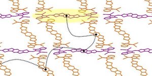
Molecular electronics (ME) is a rapidly maturing field concerned with the study of charge transport phenomena through a single molecule or an array of molecules organized between two (or more) macroscopic electrodes (Figure 1). By the careful design of the chemical structure it’s possible to study the different charge transport mechanism such as coherent tunneling and incoherent hopping and quantum interference phenomenon within the junction to achieve the functions of conventional electronic components such as chemical sensors and chemically-gated transistors (Chem-FETs), photodetectors, and thermoelectric materials.1
This presentation will describe the design and synthesis of range of linearly and cross-conjugated organic, organometallic and coordination complexes complex to study their electronic properties in the molecular junction. At the heart of this study is the exploration of the factors that influence electron transport through a molecule. In turn, this deeper understanding allows us to extend molecular design strategies beyond the search for highly conductive molecules and direct attention to more subtle concepts such as quantum interference,2 redox-gated molecular electronic response1 and the influence of the molecule-electrode contact1 and coupling to the overall electrical response of the junction (Figure 1). Molecular parameters such as the frontier orbital energy levels and HOMO-LUMO gap of the molecular candidates in their accessible redox states are therefore essential to these investigations. Therefore, in addition to the molecular junction-based measurements of molecular conductivity, investigation of the electronic structures and electrochemical properties of these molecular candidates using electrochemical, spectroelectrochemical and computational methods has also been undertaken.3

Figure 1: A schematic of a single-molecule junction, showing the conceptual features of the anchor group contacting to the electrode surface, a linking group or molecular backbone and some functional unit (e.g. a metal-ligand fragment).
The performance of the synthesised compounds to understand different charge transport mechanisms is being evaluated within scanning tunneling microscope break-junction (STM-BJ) in collaboration with Liverpool University (UK), and the theoretical calculations of molecular structure and model junctions were done in collaboration with Lancaster University (UK) and Xiamen University (China), and results will be reported.
References
1. M. Naher, D. C. Milan, O. A. Al-Owaedi, I. J. Planje, S. Bock, J. Hurtado-Gallego, P. Bastante, Z. M. Abd Dawood, L. Rincón-GarcÃa, G. Rubio-Bollinger, S. J. Higgins, N. Agraït, C. J. Lambert, R. J. Nichols and P. J. Low, J. Am. Chem. Soc., 2021, DOI: 10.1021/jacs.0c11605.
2. F. Jiang, D. I. Trupp, N. Algethami, H. Zheng, W. He, A. Alqorashi, C. Zhu, C. Tang, R. Li, J. Liu, H. Sadeghi, J. Shi, R. Davidson, M. Korb, A. N. Sobolev, M. Naher, S. Sangtarash, P. J. Low, W. Hong and C. J. Lambert, Angew. Chem. Int. Ed., 2019, 58, 18987-18993.
3. M. Naher, S. Bock, Z. M. Langtry, K. M. O’Malley, A. N. Sobolev, B. W. Skelton, M. Korb and P. J. Low, Organometallics, 2020, 39, 4667-4687.
Wednesday 7 July 2021
Seminar 1
1:00 - 1:25pm AEST
Structural origins of long-range exciton diffusion in a non-fullerene acceptor
Paul Hume
Victoria University of Wellington
In organic photovoltaic cells, absorption of light leads to the formation of excitons, which then diffuse to the donor/acceptor interface to generate photocurrent. The distance from which excitons can reach the interface is constrained by the exciton diffusion length, which has been difficult to quantitatively model or predict due to structural and energetic disorder. Modern non-fullerene acceptors have been shown to possess exceptionally large diffusion lengths, along with well-defined molecular and packing structures, suggesting that a predictive framework for materials design and computational screening may be possible.
We recently demonstrated[1] that the large diffusion coefficient observed experimentally[2] in an archetypical non-fullerene acceptor, IDIC, can be accurately quantified using density functional theory, and that the low energetic disorder means that the crystal structure provides a meaningful starting point to understand exciton motion in thin films. By accounting for short- and long-range excitonic interactions[3], as well as spatiotemporal disorder, we can accurately predict experimental values for exciton diffusivity and diffusion length. The simplicity and accuracy of this approach are directly linked to the structural order of these materials, and an electronic coupling profile that is unusually resilient to thermal distortions – highlighting the potential for computational materials screening. Moreover, we show that these factors, combined with the low reorganisation energy and significant long-range electronic coupling, lead to diffusion rates that approach the upper limit of incoherent energy transfer, and long diffusion lengths that relieve constraints on organic solar cell device architectures.
[1] P. A. Hume, W. Jiao, and J. M. Hodgkiss, J. Mater. Chem. C 2021, 9, 1419.
[2] S. Chandrabose, K. Chen, A. J. Barker, J. J. Sutton, S. K. K. Prasad, J. Zhu, J. Zhou, K. C. Gordon, Z. Xie, X. Zhan and J. M. Hodgkiss, J. Am. Chem. Soc., 2019, 141, 6922.
[3] P. A. Hume and J. M. Hodgkiss, J. Phys. Chem. A, 2020, 124, 591
Seminar 2
1:25 - 1:50pm AEST
Kiran Sreedhar Ram
Characterising Exciton Generation in Bulk-heterojunction Organic Solar Cells
The research and development in the field of organic solar cells (OSCs) have been thriving over the last few decades due to being of low cost, light weight and flexibility compared to the inorganic solar cells (ISCs). However, there are two major challenges in bringing OSCs to the commercial stage: i) low power conversion efficiency (PCE) and ii) low stability or degradation [1]. Bulk-heterojunction (BHJ) OSCs with an active layer based on fullerene acceptor have currently dominated the research activities in organic photovoltaic because of their excellent charge transport properties. However, fullerene acceptor materials have some disadvantages which include limited chemical and energetic tunability, narrow range of absorption spectra and unstable morphology thereby limiting the overall PCE and stability of the devices thus fabricated. Therefore, the research focus has moved to the use of non-fullerene (NF) acceptors in BHJ OSCs. In this research, work has been done in understanding the characteristics of exciton generation in conventional and inverted NF acceptor based BHJ OSCs and the results are also compared to fullerene acceptor based BHJ OSCs. [2]
The characterisation of exciton generation is carried out in three BHJ OSCs, OSC1: an inverted NF BHJ OSC, OSC2: a conventional NF BHJ OSC and OSC3: a conventional fullerene BHJ-OSC. It is found that the overlap of the regions of strong constructive interference of incident and reflected electric fields of electromagnetic waves and those of high photon absorption within the active layer depends on the active layer thickness. An optimal thickness of the active layer can thus be obtained at which this overlap is maximum. We have simulated the rates of total exciton generation and position dependent exciton generation within the active layer as a function of the thicknesses of all the layers in all three OSCs and optimised their structures. Based on our simulated results, the inverted NF BHJ OSC1 is found to have better short circuit current density which may lead to better photovoltaic performance than the other two. [2]
[1] K. S. Ram and J. Singh, “Highly Efficient and Stable Solar Cells with Hybrid of Nanostructures and Bulk Heterojunction Organic Semiconductors,†Advanced Theory and Simulations, vol. 2, no. 6, p. 1900030, 2019/06/01 2019, doi: 10.1002/adts.201900030.
[2] Sreedhar Ram K, Mehdizadeh-Rad H, Ompong D, Setsoafia DDY, Singh J. Characterising Exciton Generation in Bulk-Heterojunction
Wednesday 2 June 2021
Seminar 1
1:00 - 1:40pm AEST
Inelastic Neutron Scattering as a tool for investigating organic semiconductors
Richard A. Mole
Australian Centre for Neutron Scattering, ANSTO
Inelastic neutron scattering is a unique tool for probing vibrations and diffusion both in terms of the energy but also on a spatial scale. This has allowed it to be used as a powerful tool for materials characterisation for the past fifty years.
In this seminar I will introduce the technique of inelastic neutron scattering and provide an overview of the instrumentation currently available to the Australian research community. I will use several examples of work that has been performed both on the instruments at ANSTO and around the world to demonstrate how this may be a tool of use for the AUCAOS community (eg 1,2)
[1] H. Cavaye, Angewandte Chemie, 2018, 131, 28
[2] A.Y. Guilbert, M. Zbiri, P.A. Finn, M. Jenart, P. Fouquet, V. Cristiglio, B. Frick, J. Nelson, C.B. Nielsen Chem. Mater, 2019, 31, 9635
Wednesday 5 May 2021
Seminar 1
1:00 - 1:25pm AEST
The Effects of Deposition Technique on Charge and Exciton Dynamics in OLEDs – A Computational Study
Stephen Sanderson
James Cook University & The University of Queensland
Solution-processed OLED films present a number of advantages in cost and scalability over their vacuum-deposited counterparts. However, they currently do not meet the same performance standards, tending to degrade at a faster rate. Towards understanding this, kinetic Monte-Carlo transport modelling combined with molecular dynamics deposition modelling offers a detailed picture of device operation, and allows for the establishment of structure-property relationships that can be difficult to observe through other means. This presentation gives an overview of KMC modelling techniques in the context of phosphorescent OLEDs, along with an outline of techniques developed for building thicker solution-deposited films without the need for prohibitively large initial systems. Using these techniques, a comparison is made between charge and exciton dynamics in solution- and vacuum-deposited OLED films with the goal of gaining insight into the cause of experimentally observed differences in degradation rate.
Seminar 2
1:25 - 1:50pm AEST
Ternary Strategy and Burn-in Degradation Investigation of Organic Solar Cells
Leiping Duan
The University of New South Wales
Organic solar cells (OSCs) as a low-cost new generation of renewable energy technology have become a promising contender that could serve as an alternative to silicon to established photovoltaic (PV) technologies in the future. Meticulous active layer engineering is a crucial element for OSCs to improve the device performance, where the application of the ternary strategy is an effective pathway. The ternary strategy retains the simplicity of the fabrication for organic solar cells and exhibits a higher potential towards large-scale fabrication. Investigating the novel application of ternary strategy in OSCs is a promising method towards higher device performance. Apart from the pursuit of the device performance, research for the long-term OSCs device stability is also critical for its practical applications and future commercialization. Burn-in degradation has become an ineluctable barrier for OSCs to achieve long-time stability, where an in-depth understanding of the mechanism behind burn-in degradation has become the precondition to conquer this barrier. The aim of research works in my PhD thesis is to improve the performance of OSCs and provide understandings of its degradation mechanism behind. The ternary strategy, especially incorporated with novel non-fullerene acceptor materials, as a performance improving method, is the primary focal point in this thesis. In this thesis, we derived three novel ternary OSCs and provided a comprehensive investigation of the mechanism behind its performance enhancement. On the other hand, this thesis also systematically investigated the burn-in degradation mechanism in OSCs. We analysed the degradation mechanism based on each instability factor including light, heat, and air, to gain in-depth understating. Moreover, combined with the application of ternary strategy and the burn-in degradation study, we did a case study of the burn-in degradation in the high-efficiency PTB7-Th: COi8DFIC: PC71BM ternary OSCs. We found that the ternary strategy could increase the stability of the device, and the burn-in degradation mechanism in ternary OSCs is more dependent on its dominant binary counterpart. Overall, insights gained in this work into the nature of ternary strategy and burn-in degradation provide a step for OSCs towards large scale application and future commercialization.
Wednesday 7 April 2021
Seminar 1
1:00 - 1:25pm AEST
Organic Polariton Lasing with Molecularly Isolated Perylene Diimides
Dr. Girish Lakhwani
Sydney University
In the last decade, strong light matter coupling has become an alternative path to achieve lasing in organic materials via use of polaritons. Polariton lasers do not require population inversion and thus hold the promise of lower laser thresholds. Organic materials are particularly suited for polariton lasing as their large absorption coefficients result in impressive exciton-photon couplings strengths at room temperature. Here I will demonstrate polariton lasing in a molecularly isolated perylene diimide. [1,2] The emission exhibits threshold behaviour, spatial coherence, and the characteristic blue-shifting of polariton systems. We expect perylene dyes will become a useful polariton laser class.
1. Sabatini et al. J Mater Chem C, 7, 2954 (2019)
2. Sabatini et al. Appl. Phys. Lett, 117, 041103 (2020)
Seminar 2
1:25 - 1:50pm AEST
Optimal quantum dot size for photovoltaics with fusion
Dr. Laszlo Frazer
Monash University
Light fusion increases the efficiency of solar cells by converting photons with lower energy than the bandgap into higher energy photons. The solar cell converts the produced photons to current. We use Monte Carlo simulation to predict that lead sulfide quantum dot sensitizers will enable fusion with a figure of merit on the mA/cm^2 scale, exceeding current records, while enabling silicon cell compatibility. Performance is highly sensitive to quantum dot size, on the order of mA/cm^2/nm.
Wednesday 10 March 2021
Seminar 1
1:00 - 1:25pm AEST
N-Heterocyclic Carbene Platinum(II) Dialkynyl Complexes - A New Class of Highly Tunable and Efficient Emitter Systems
Assoc. Prof. Koushik Venkatesan
Macquarie University
New and efficient light-emitting materials are required for a broad range of potential applications in the fields of sensors, storage, photoelectronic devices, and optical devices. Extensive investigations on transition metal complexes as triplet emitters for application in phosphorescent organic light emitting devices (PhOLEDs) have been carried out. Metal complexes with specific ligand environment allow to tailor the luminescent properties in a precise fashion for a specific application. Achieving high stability, high quantum efficiency and specific chromaticity remains a major challenge in this field. Recently, our group has demonstrated a series of highly emissive platinum(II) complexes bearing N-heterocyclic carbene ligands with promising photophysical properties. Further building on this work, we have developed new series of small molecules and investigated their detailed luminescent properties. Selected molecules that have been fabricated into devices show high potential for applications in light emitting devices.
Seminar 2
1:25 - 1:50pm AEST
Classification of Coherent Enhancements of Light-Harvesting Processes
Assoc. Prof. Ivan Kassal
The University of Sydney
Several kinds of coherence have recently been shown to affect the performance of light-harvesting systems, in some cases significantly improving their efficiency. Recently, we classified the possible mechanisms of coherent efficiency enhancements [1], based on the types of coherence that can characterize a light-harvesting system and the types of processes these coherences can affect. We show that enhancements are possible only when coherences and dissipative effects are best described in different bases of states. In addition, our classification allows us to predict a previously unreported coherent enhancement mechanism.
I will discuss the implications of this classification for the field of organic photovoltaics. Several coherent mechanisms have been proposed for boosting OPV efficiency, but most of them are impossible. A few manifestations of coherence may matter, including one that we are confident plays a big role in OPV performance [2].
[1] Stefano Tomasi and Ivan Kassal, J. Phys. Chem. Lett. 2020, 11, 2348 - 2355.
[2] Daniel Balzer, Thijs J.A.M. Smolders, David Blyth, Samantha N. Hood, and Ivan Kassal, Chem. Sci. doi:10.1039/D0SC04116E (2021).
Wednesday 3 February 2021
Seminar 1
1:00 - 1:25pm AEST
A flexible organic solar cell based on doped graphene/PET substrate
Hellen Jin
The University of Queensland
Graphene has shown tremendous potential as a transparent conductive electrode (TCE) for flexible organic solar cells (OSCs). However, the trade-off between electrical conductance and transparency as well as surface roughness of the graphene TCE with increasing layer number limits power conversion efficiency (PCE) enhancement and its use for large-area OSCs. Here, we use a 300 nm-thick poly[(2,5-bis(2-hexyldecyloxy)phenylene)-alt-(5,6-difluoro-4,7-di(thiophen-2-yl)benzo[c]-[1,2,5]thiadiazole)]:[6,6]-phenyl-C71-butyric acid methyl ester as the photoactive layer and a benzimidazole (BI)-doped graphene as the transparent anode to demonstrate efficient OSCs with good flexibility. It is found that 3 layer (L) graphene had the best balance between sheet resistance, optical transmittance and surface roughness for optimized cell design. A 0.2 cm2 cell with a 3L BI-doped graphene anode achieves a PCE of 6.85%, which is one of the highest PCE values reported so far for flexible graphene anode-based OSCs. The flexible cells are robust, showing only a small performance degradation during up to 250 flexing cycles. Moreover, the combination of the thick photoactive layer with the optimized 3L BI-doped graphene TCE enabled production of 1.6 cm2 flexible OSCs with a PCE of 1.8%. Our work illustrates the importance of graphene TCE development for flexible OSCs as well as other wearable optoelectronic devices.
Seminar 2
1:25 - 1:50pm AEST
Carbene-metal-amides as emitting materials in high-efficiency organic light-emitting diodes
Patrick Conaghan
University of Sydney / University of Cambridge
Emitting materials in organic light-emitting diodes are predominantly phosphorescent iridium complexes or all-organic thermally activated delayed fluorescence materials. We have demonstrated that the carbene-metal-amide molecular structure of coinage-metal complexes can also be used to produce organic light-emitting diodes with efficient electroluminescence from both singlet and triplet excited states. We have shown that the emission colour can be changed through variation of the electron-donating strength of the donor moiety and the polarity of the host environment and have used both of these effects to produce devices with emission across the visible range. By engineering excited state energies we have fabricated green-emitting devices with a maximum electroluminescence quantum efficiency of 26.9 % and blue-emitting devices (Commission Internationale de l'Éclairage co-ordinates [0.17, 0.17]) with external quantum efficiency of 20.9 %. Transient photoluminescence measurements at varying temperatures show that the emission process is thermally activated with short excited-state lifetimes (<1 μs) and along with device data show that the energy of local triplet excited states imposes an energy limit on efficient emission. Carbene-metal-amides do not show a strong concentration-dependent luminescence quenching in the solid state, which has allowed us to fabricate host-free devices with external quantum efficiency of up to 23 % which, to our knowledge, is the highest reported for host-free organic light-emitting diodes.
Wednesday 2 December 2020
Seminar 1
1:00 - 1:25pm AEST
Non-Toxic Hybrid Inorganic-Organic Chromophores for the Advancement of Luminescent Solar Concentrators
Calum Gordon
Victoria University of Wellington
Luminescent solar concentrators (LSCs) consist of a waveguide medium containing light harvesting chromophores of an inorganic or organic nature. These chromophores absorb incoming light, and radiatively re-emit light, which is propagated to the edges of the LSC by the waveguide. The concentrated light at the edges is then collected by coupled solar cells.
The advantages of LSCs coupled to solar cells relative to stand alone solar cells are that LSCs are cheaper, and can capture indirect sunlight.
A pressing issue with modern LSCs are re-absorption events by the chromophore, which dampens their efficiency. This is due to overlap between the absorbance and emission spectra of the chromophore.
By coupling inorganic and organic components together, Förster resonance energy transfer (FRET) may be achieved between the two components, creating a donor-acceptor system. The donors absorbance spectrum is sufficiently separated from the acceptors emission spectrum, mitigating re-absorption events.
Seminar 2
1:25 - 1:50pm AEST
Magnetic field effect on UC-TTA
Elham Gholizadeh
The University of New South Wales
Solar light contains many wavelengths, but solar cells cannot absorb all those wavelengths. In fact, those photons which do not have enough energy to be absorb by the band gap will be wasted. One of the strategies that have been used until now in terms of using low energy photons is Triplet-Triplet Annhilation upconversion (UC-TTA). In this process two low energy photons will convert to a higher energy photon.
In terms of improving solar cells efficiency, it is important to make an upconversion system which convert photons below the bandgap to the photons that absorb by the solar cell. Also, since most of the upconversion system does not work in oxygen environment, finding a solution for this problem looks essential.
In my PhD, I could do UC-TTA from below the silicon bandgap in oxygen mediated environment. In this system, opposite other UC-TTA systems, oxygen improves the upconversion efficiency. So, in terms of understanding the mechanism of UC-TTA in our system in the presence of oxygen, magnetic field effect on TTA process was used. We also considered magnetic field effect on two well known UC-TTA system to be able to modify Merrifield equation and the data was fitted by this equation.
Wednesday 4 November 2020
Seminar 1
1:00 - 1:25pm AEST
Partial Delocalisation Enhances the Efficiency of Charge Separation in Organic Photovoltaics
Daniel Balzer
University of Sydney
In organic photovoltaics, the question of how charges are able to overcome their significant coulombic attraction and separate has attracted heated debate. In particular, the low dielectric constants in organic semiconductors produce coulombic barriers that are an order of magnitude greater than the available thermal energy. One of the proposed answers is delocalisation, including arguments that the increased separation of charges in the CT state reduces the coulombic barrier. However, it turns out that delocalisation stabilises the CT state and increases the coulombic barrier, and therefore any benefit provided by delocalisation must come from non-equilibrium kinetic effects. However, charge separation is a two-body problem involving the correlated motion of an electron and a hole, meaning that the computational difficulty is roughly the square of the single-body mobility calculation, meaning that a fully quantum-mechanical treatment has so far proved intractable in three dimensions. A complete kinetic model would help settle the debate about the main drivers of charge separation, and unite the proposed mechanisms including delocalisation, entropy and energy gradients. Last year, we presented delocalised kinetic Monte Carlo (dKMC), the first three-dimensional model of partially delocalised charge and exciton transport in materials in the intermediate disorder regime. Here, we use dKMC to make the charge separation problem computationally accessible, allowing the first simulation of the full dynamics (and, therefore, efficiency) of charge separation in the presence of disorder, delocalisation, polaron formation and noise. We find that small amounts of delocalisation can produce large enhancements in the efficiency at which charges separate.
Seminar 2
1:25 - 1:50pm AEST
Spatially Correlated Quantum Properties in Organic Light Emitting Diodes
William Pappas
The University of New South Wales
Electronic spin is a quantum mechanical property that is fundamental to the charge-light conversion processes in optoelectronic devices. The suppression of interactions between spins in organic semiconductors leads to relatively long relaxation times (?s) and results in the formation of weakly coulombically bound electron-hole pairs. The ability to access and modulate the spin polarisation of these pairs enhances the quantum efficiencies of device DC observables (current, luminosity), while also enabling unique functionality in spin-logic devices. In organic light-emitting diodes, the study of spin-dependent processes giving rise to magnetic field effects have been treated monolithically. We have incorporated optical imaging microscopy into a traditional magneto-electroluminescence (MEL) setup that has allowed us to discern the intra-device variation of the quantum property (hyperfine interaction) which is responsible for these effects. We investigated the correlations between these local hyperfine field strengths in both the spatial and temporal domains. Magnetic resonance measurements are then used explain the origin of variations in the MEL lineshapes. This work is an important step in characterising the homogeneity of spin-dependent properties in organic materials which critically control the ability to manipulate spins in organic spintronic devices.
Wednesday 7 October 2020
Seminar 1
1:00 - 1:25pm AEST
Understanding the interplay between charge transport, luminescence efficiency and morphology in OLEDs using a combined computational & experimental approach
Mile Gao
University of Queensland
Phosphorescent emissive materials in organic light-emitting diodes (OLEDs) manufactured using evaporation are usually blended with host materials at a concentration of 3–15 wt% to avoid concentration quenching of the luminescence. In this work, experimental measurements of hole mobility and photoluminescence are related to the atomic level morphology of films created using atomistic nonequilibrium molecular dynamics simulations mimicking the evaporation process with similar guest concentrations as that used in operational test devices. It was found that the photophysical and charge transport properties of the film have significantly different guest–guest distance dependence.
Seminar 2
1:25 - 1:50pm AEST
The effect of gate conductance on hygroscopic insulator organic field effect transistors
Joshua Arthur
Queensland University of Technology
Organic thin film transistors (OTFTs), employing a variety of device architectures, materials, and transduction mechanisms, have shown great promise as effective chemical and biological sensors. One such class of OTFT is the hygroscopic insulator field effect transistor (HIFET). HIFETs utilise a hygroscopic polymer dielectric that behaves as a solid-state electrolyte, facilitating low voltage (<1 V) operation, in a simple, solution processable, solid-state form factor. Sensitivity to various analytes can be achieved by modifying the top gate electrode with appropriate porous membranes or recognition elements. However, a change to the electrical properties of the gate electrode can significantly degrade transistor characteristics. To better understand this behaviour, we have explored the effect of gate conductance on HIFET performance, using PEDOT:PSS films of varied thickness as a model gate electrode. As gate conductance increases, key figures of merit including ON/OFF ratio, threshold voltage and transconductance improve until approaching a plateau. We understand this effect in terms of a change in the magnitude of the effective gate voltage. These results imply widely applicable design rules, where good transistor functionality can be achieved with a range of gate conductance values that lie in the plateau region, allowing flexibility to incorporate poorly conducting materials that facilitate sensitivity.
Wednesday 2 September 2020
Seminar 1
1:00 - 1:25pm AEST
Nanoscale Capacitor-like Field Buildup Reveals Charge Protection in an Organic Heterojunction
Dr Kyra Schwarz
University of Melbourne
Emerging thin-film solar technologies often comprise nanoscale structural complexity that dramatically impacts the efficiency of light harvesting. Researchers have long considered how to suppress the loss of free carriers by recombination, an effect that is intimately connected to local morphology in the donor-acceptor heterojunctions of organic solar cells. Using femtosecond transient spectroscopies, we report the nanosecond grow-in of a large transient Stark effect, caused by nanoscale electric fields of ~487 kV/cm between photogenerated free carriers in the device active layer. We find that particular morphologies of the active layer lead to an energetic cascade for charge carriers, which in turn leads to the local build-up of electric charge that is resistant to bimolecular recombination and consistent with higher device efficiencies. These observations suggest that with particular nanoscale morphologies the bulk heterojunction can go beyond its established role in charge photogeneration and can act as a network of tiny capacitors, where adjacent free charges are held away from the interface and can be protected from bimolecular recombination.
Seminar 2
1:25 - 1:50pm AEST
Design and Application of TADF Emitters for Blue and White OLEDs
Dr. Andrew Danos
Durham University
Thermally activated delayed fluorescence has allowed all-organic OLED emitters to reach the high efficiencies previously reserved by organometallic phosphors. Rapid reverse intersystem crossing (rISC) converts non-radiative triplet excitons into emissive singlets in devices, enabled by vibronic coupling of excited states with different multiplicity and orbital character. However this approach is not without drawbacks, and the complexity of the rISC process along with its strong sensitivity to host environment make it challenging to successfully design and implement blue and deep-blue TADF emitters. Despite these challenges, recent progress in this area has been rapid. In this talk I will outline the general structural features required to design TADF materials, along with the experimental techniques used to screen and characterise their performance. Recent work applying external downconversion layers will also be presented, in which a high performance blue TADF OLED is modified to give white emission without loss of efficiency.
Wednesday 5 August 2020
Seminar 1
1:00 - 1:25pm AEST
Characterising the Interface and Dipole in Organic-based Photovoltaics
Dr. Yanting Yin
Flinders University
A combination of electron spectroscopy and ion scattering spectroscopy has been carried out to directly characterize the chemical and electrical properties at the interface formed with high workfunction (WF) hole transport layer-MoO3 and conjugate polymer. Characterization of chemical features and concentration distribution on a P3HT:PC61BM bulk-heterojuction (BHJ) with MoO3 arises an observation of energy shift of BHJ and diffusion of MoO3. The dipole formation at such interface can be indicated. Gradual changes upon electronic structure such as WF and valence electron states were observed from the analysis. A decomposition algorithm introduced in the work yields an insight into the dipole strength thus the complete energy level positioning at the interface can be restored. The mechanism of charge transport over the MoO3/BHJ interface was thus discussed with the determination of dipole strength maximizing at 2.1eV. A similar characterization upon interface was studied upon the growth of thermal-evaporated LiF on polymer BHJ. Further investigation has been made of the interface with a simulation of common contamination such as air exposure, and commercialized fabrication process such as thermal annealing consequence during fabrication. The results show that, the electronic properties of the original interface can be altered once the structure was subjected to contamination and thermal treatment. The analysis offers an insight of device performance of solar cells correlated to interface dipole features.
Seminar 2
1:25 - 1:50pm AEST
Red Emission from Nature Inspired Bay-Annulated Indigo Derivatives
Ms Nicholle Wallwork 1,2
University of Queensland
Atul Shukla,1,3 Xin Li,1,2 Jan Sobus,1,3 Van T. N. Mai,1,2 Sarah K. M. McGregor,1,2 Kay Chen,2 Romain J. Lepage,2 Elizabeth H. Krenske,2 Evan G. Moore,2 M. Mamada,4 C. Adachi,4,* Ebinazar B. Namdas,1,3* Shih-Chun Lo1,2*
1. Centre for Organic Photonics & Electronics, The University of Queensland, Brisbane, Queensland, 4072, Australia
2. School of Chemistry and Molecular Biosciences, The University of Queensland, Brisbane, Queensland, 4072, Queensland, Australia
3. School of Mathematics and Physics, The University of Queensland, Queensland, Brisbane, Queensland, 4072, Australia
4. Centre for Organic Photonics and Electronics Research (OPERA), Kyushu University, 744 Motooka, Nishi, Fukuoka 819-0395, Japan
Organic semiconductor materials offer high mechanical flexibility and high wavelength-tunability, which have great potential as a complementary technology to current inorganic lasers, particularly for spectroscopy, sensing, optical data communication, display, and security tag applications.1 Recent research efforts on organic semiconductor lasers have demonstrated notable organic semiconductor materials possessing both high optical gain and low amplified spontaneous emission (ASE) thresholds in blue and green colours.2 However, the same progress has not been made on red laser dyes mainly due to their low photoluminescence quantum yields (PLQYs) recognised as the “energy bandgap law†for low-energy emission.
To overcome this, in this presentation our development of a new family of solution-processable organic semiconductor laser dyes with deep-red emission, high thermal stability and high PLQYs (≈100%) will be shown. Our strategies in achieving low film ASE thresholds (9.6 μJ/cm2 at 650 nm), low laser thresholds (6 μJ/cm2) and high stability under optical pumping (retained 90% of the initial output even after (≈9,600 pump pulses of continuous pumping at 20 Hz) will be further discussed.3 Finally, our preliminary work on TADF-Assistant Fluorescent OLEDs (TAF-OLEDs)4 based on the new red laser dyes will be demonstrated to show high promise as a new family of organic semiconductor materials.

References:
1. A. J. C. Kuehne, M. C. Gather., Chem. Rev. 2016, 116, 12823.
2. T. N. V. Mai, A. Shukla, M. Mamada, S. Maedera, P. E. Shaw, J. Sobus, I. Allison, C. Adachi, E. B. Namdas, S.-C. Lo, ACS Photonics 2018, 5, 4447; Y. Oyama, M. Mamada, A. Shukla, E. G. Moore, S.-C. Lo, E. B. Namdas, C. Adachi, ACS Mater. Lett. 2020, 21, 161.
3. A. Shukla, N. R. Wallwork, X. Li, J. Sobas, V. T. N. Mai, S. K. M. McGregor, K. Chen, R. J. Lepage, E. H. Krenske, E. G. Moore, E. B. Namdas, S.-C. Lo, Adv. Opt. Mater. 2020, 8, 1901350.
4. H. Nakanotani, T. Higuchi, T. Furukawa, K. Masui, K. Morimoto, M. Numata, H. Tanaka, Y. Sagara, T. Yasuda, C. Adachi, Nature Commun. 2014, 5, 4016.
Acknowledgement: We thank Australian Research Council (DP160100700 and DP180103047), and Department of Industry, Innovation and Science (AISRF53765), and Japan Society for the Promotion of Science (JSPS Core-to-Core 18050011-000441) for financial support.
Thursday 2 July 2020
Seminar 1
1:00 - 1:25pm AEST
Hybrid organic/inorganic chromophores
Dr Nathaniel Davis
Victoria University of Wellington
Luminescent light harvesting chromophores have the potential to improve many optoelectronic technologies, such as photovoltaics, LEDS, lasers and luminescent solar concentrators. Our research into the creation of artificial light-harvesting antenna complexes aims to disrupt the current chromophore technology. The current state of the art chromophores can be split into two types: 1) Organics, which suffer heavily from instability and reabsorption; and 2) Inorganics, which solved many of the problems inherent with organic emitters in terms of stability and reabsorption but require complex surface treatments to improve their luminescent efficiency (LE). We aim to combine the beneficial properties of both these systems into a single hybrid chromophore. This will act to improve the LE of the hybrid particle and reduce reabsorption losses. The science behind attaching chromophores to nanocrystals and studying the subsequent photophysics is in its infancy. We envision two options forward, that would promote the field, both based on the replacement of ligands on a nanocrystal that offer colloidal stability with ones that add additional optoelectronic properties. 1) Energy transfer from the ligand into the nanocrystal, which will have potential applications for increased solar absorption, efficient transport of excitations, and singlet fission. 2) Coupling a highly luminescent molecule to a nanocrystal, avoids the complex surface passivations (treatments) required by current state-the-art nontoxic emitters and offers the potential for upconversion of light.This talk will look at our recent success with caesium lead halide nanocrystals.
Seminar 2
1:25 - 1:50pm AEST
Dicyanovinyl-based fluorescent sensors for dual mechanism amine sensing
Dr. Guanran Zhang
University of Queensland
Food wastage due to spoiling is a global economic issue and contributes to over-farming and overfishing with real environmental consequences. Smart food packaging is a promising solution to this problem, the idea of which is to utilize responsive sensors that allow direct monitoring of the gasses released from food as it spoils and provides a visual indicator to the consumer. Here we report two dicyanovinyl-fluorene-benzothiadiazole-based fluorescent compounds, K12 and K12b, both of which showed rapid response to biogenic amines via two independent mechanisms. When primary alkyl amines were present in solution, they underwent Michael addition with the dicyanovinyl group of the sensing material, resulting in rapid color change. The reaction products of K12 and K12b with primary amines also showed a decrease and increase in the fluorescence quantum yield, respectively, enabling a unique dual-sensor array with turn-off/turn-on response. In addition, fluorescence quenching via photoinduced hole transfer was observed in the solid-state sensor films with a wide range of primary, secondary and tertiary amines, enabling rapid and sensitive detection of amine vapors. Finally, as a proof-of-concept integrated packaging sensor, soft membranes incorporating K12 and K12b were prepared and showed rapid response to primary amine vapor.
Thursday 4 June 2020
Seminar 1
1:00 - 1:25pm AEST
An introduction into synthetic molecular motors
Dr Jos Kistemaker
The University of Queensland
Scientific advances made in the last three decades, inspired by Nature's example, has led to a diverse collection of synthetic molecular machinery. A prominent example of this machinery is the molecular motor developed by Feringa and co-workers which is based on a light driven overcrowded alkene. The study of several generations of molecular motors and their properties have had primarily academic merit, however, later developments have shown that these nanomachines can be used to do actual work and might prove to be the driving force in the transition to actual applications.
This talk will provide an introduction into the field of synthetic molecular motors with an emphasis on light driven rotary motors. The role of autonomy and chirality in different designs will be highlighted and several examples will be used to showcase the expression and translation of these features to other groups, molecules and larger scales.
Seminar 2
1:25 - 1:50pm AEST
Electronic coupling: A significant contributor to electron transfer between similarly structured surface-bound porphyrins and Co2+/3+ complex electrolytes
Mr Inseong Cho
University of Wollongong
Electronic coupling is often assumed to play a minor role in interfacial electron transfer (ET) between similarly structured electron donors and acceptors. To check this assumption, we investigated the ET kinetics between four surface-bound free-base and Zn porphyrins and five Co2+/3+ complexes redox mediators with different ligands using transient absorption spectroscopy (TAS). The ET rates measured in this work are the fastest reported in the literature for surface-bound molecules and donors dissolved in electrolytes. By using a novel sub-ns TA setup, the importance of enhanced TAS time-resolution is demonstrated. Fitting the measured ET rate versus -ΔG resulted in poor fits with unrealistic trends in reorganisation energy values. This is explained by up to 60% variation of the electronic coupling (HDA) depending on the size of the alkyl-substituent of the Co2+/3+ complexes redox mediator. The HDA values obtained by assuming a constant reorganisation energy are shown to be dependent on tunnelling distances, characterised by tunnelling attenuation factor βel = 0.16 to 2.0 Å-1. This work suggests that changes in electronic coupling even by small structural modification previously considered negligible can be as significant as the effect of driving force.
Thursday 7 May 2020
Seminar 1
1:00 - 1:25pm AEST
Microstructure formation in solution-processed semiconducting polymer thin films
Prof. Chris McNeill
Monash University
Semiconducting polymers are interesting materials that are being developed for a wide range of applications including polymer field-effect transistors, polymer solar cells, and polymer light emitting diodes. The performance of such devices is strongly dependent upon the thin film microstructure of the active semiconducting polymer thin film. As semiconducting polymers are processed from solution, the resulting thin film microstructure is complicated and can be hard to control. In this presentation I will present research performed in my group aimed at understanding how microstructure forms in solution-processed semiconducting polymer thin films. A focus will be placed on the n-type naphthalene dimide-based polymer P(NDI2OD-T2) which exhibits a rich microstructure and good performance in field-effect transistors and polymer solar cells. The influence of molecular weight and processing conditions on thin film microstructure will be discussed, along with the impact of thin film microstructure on field-effect transistor performance. This talk will also feature a host of different synchrotron-based techniques that have been used to understand the polymer physics and microstructure of this system.
Seminar 2
1:25 - 1:50pm AEST
Charge transport in disordered materials for photodetector applications
Dr. Almantas Pivrikas
Murdoch University
Non-crystalline disordered semiconductors such as organic molecules, polymers, nanoparticles offer great advantage for electronic devices where the novel physics as well is yet to uncovered. All these materials lack long range structural order and have one common feature - their electrical conduction is inferior compared to highly-crystalline inorganic semiconductors such as silicon because of orders of magnitude lower electron and hole mobilities as well as strong recombination rates. Yet, organic electronic devices made using these disordered materials have the performance comparable to their classical inorganic counterparts. Photoconductivity and charge transport measurement techniques such as Time-of-Flight or Hall-effect are typically not applicable or unreliable to study the charge transport in these disordered systems. In this presentation the core problems with experimental issues will be explained and our novel techniques introduced. Our work relating to hot photocarrier utilization in photodetectors as well as the novel peculiarities of charge carrier recombination in crystalline and disordered semiconductors will be demonstrated.